Zero-Defect Approach in PCBA Manufacturing
Electronic assembly (PCBA) is a high-tech process in which micron-level tolerances and sensitive chemical/thermal reactions are managed. Shrinking board sizes, narrowing component pitches, and the increasing use of microscopic packages like BGA/QFN max the risk of defects during assembly. In this article, we examine the challenges we face in our modern manufacturing facilities equipped with Novenix and Solderprof engineering and how we overcome them.
1. Solder Paste Printing Precision and Stencil Design
Approximately 60% of PCBA manufacturing defects occur during the solder paste printing phase. Insufficient solder leads to cold solder joints or opens, while excessive solder leads to short circuits (bridging). To overcome this, we use laser-cut steel stencils, custom thickness transitions (step-down stencils), and automated solder paste inspection (SPI) systems.
2. Reflow Profile Optimization
Components of different masses on the board (like small resistors versus large transformers) absorb heat at different rates during reflow. Incorrect thermal profiles cause components to fail due to overheating or result in unsoldered joints. In our facilities, we prevent thermal stress by performing multi-zone thermal profiling customized for each board.
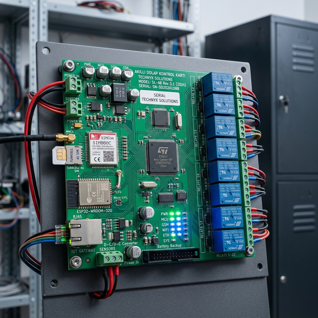
3. Thermal Shock in THT Components and the THT Soldering Machine Advantage
On double-sided boards containing SMD components that have already gone through reflow, soldering THT (through-hole) components poses a major risk. Wave or manual soldering can cause SMD components to reflow again or crack due to thermal shock. With our Solderprof THT soldering machine robots, we apply localized heat only to the target pins, eliminating this risk entirely. For detailed manufacturing processes, you can review our SMD and THT Assembly page.
4. Quality Control: AOI and Functional Testing (FCT)
Every single board manufactured is checked at a micron level by our Automated Optical Inspection (AOI) devices. Then, using custom-designed test fixtures and software, all functions of the boards (current draw, communication signals, input-output ports) are tested to ensure zero-defect packaging.
Conclusion
Quality in electronic card manufacturing is not a coincidence; it is the result of meticulous engineering and advanced machinery. To realize your projects with a zero-defect target, you can contact us and start working with our expert team.